(China (Mainland))

Product Summary
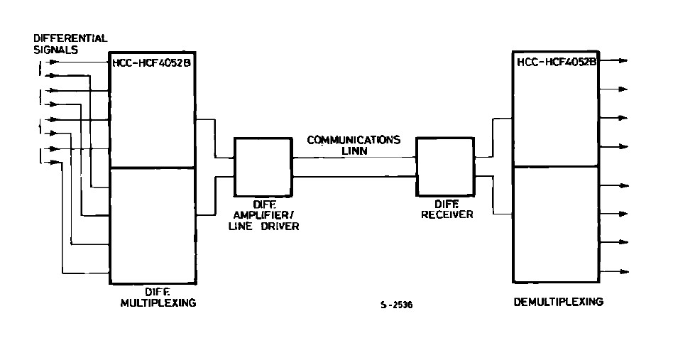
The HCF4053BE is a monolithic integrated circuit, available in 16-lead dual in-line plastic or ceramic package and plastic micropackage. The HCF4053BE analog multiplexer/demultiplexer is digitally controlled analog switches having low ON impedance and very low OFF leakage current. The multiplexer circuit dissipate extremely low quiescent power over the full VDD –VSS and VDD –VEE supply-voltage ranges, independent of the logic state of the control signals.When a-logic "1" is present at the inhibit input terminal all channel are off. The HCF4053BE is a single 8-channel multiplexer having three binary control inputs, A, B, and C, and an inhibit input. The three binary signals select 1 of 8 channels to be turned on, and connect one of the 8 inputs to the output. The HCF4053BE is a differential 4-channel multiplexerhaving twobinary control inputs, Aand B,and an inhibit input. The two binary input signals select 1 of 4 pairs of channels to be turned on and connect the analog inputs to the outputs. The HCF4053BE is a triple 2-channel multiplexer having three separate digital control inputs, A, B, and C, and an inhibit input. Each control input selects one of a pair of channels which are connected in a singlepole double-throw configuration.
Parametrics
HCF4053BE absolute maximum ratings: (1)Vi Input Voltage – 0.5 to VDD + 0.5 V; (2)II DC Input Current (any one input) ± 10 mA; (3)To p Operating Temperature : HCC Types – 55 to + 125℃; (4)HCF Types: – 40 to + 85℃; (5)Ts tg Storage Temperature: – 65 to + 150 ℃; (6)Pt ot Total Power Dissipation (per package) Dissipation per Output Transistor: 200 mW; (7)for Top = Full Package-temperature Range: 100mW.
Features
HCF4053BE features: (1)Quiescent current specified TO 20V for hcc device ; (2)low "ON" resistance : 125W (typ.) OVER 15V p.p. Signal-input range for VDD VEE = 15V; (3)High "off" resistance : CHANNEL LEAK AGE ± 100pA (typ.) VDD – VEE = 18V; (4)Binary addressdecodingon chip; (5)Very low quiescent power dissipation under all digital control input and supply conditions : 0.2 mW (typ.), VDD – VSS = VDD – VEE = 10V; (6)Matched switch characteristics: Ron = 5W (typ.) for VDD – VEE= 15V; (7)Wide range of digitaland analog signallevels: Digital3 TO 20V, analog to 20V p.p; (8)5V, 10V, AND 15V parametric ratings; (9)Input current of 100mA AT 18V AND 25℃ for HCC device; (10)100% testedfor quiescent current Meetsallrequirementsofjedectentative standard No 13A, standard specifications for description of "B" seriescmos devices.
Diagrams
| Image | Part No | Mfg | Description |  |
Pricing (USD) |
Quantity | ||||||||||||||||||
|---|---|---|---|---|---|---|---|---|---|---|---|---|---|---|---|---|---|---|---|---|---|---|---|---|
 |
 HCF4053BEY |
STMicroelectronics |
Multiplexer Switch ICs 2-Ch Ana Mult/Demult |
Data Sheet |
|
|
||||||||||||||||||
| Image | Part No | Mfg | Description | |
Pricing (USD) |
Quantity | ||||||||||||||||||
 |
HCF4001B |
Other |
|
Data Sheet |
Negotiable |
|
||||||||||||||||||
|
HCF4001BEY |
STMicroelectronics |
Gates (AND / NAND / OR / NOR) Quad 2-Input NOR |
Data Sheet |
|
|
||||||||||||||||||
 |
HCF4001M013TR |
|
IC GATE NOR QUAD 2INP 14-SOIC |
Data Sheet |
|
|
||||||||||||||||||
|
HCF4002B |
Other |
|
Data Sheet |
Negotiable |
|
||||||||||||||||||
|
HCF4006B |
Other |
|
Data Sheet |
Negotiable |
|
||||||||||||||||||
|
HCF4007UB |
Other |
|
Data Sheet |
Negotiable |
|
||||||||||||||||||